原始的VPR架构

原始的VPR架构如图所示,是一个同构的FPGA,仅仅只包含CLB(包含四个BLE,和一个全连接的crossbar)和IO。其中每个BLE包含一个四输入的查找表、一个触发器以及一个二选一多路选择器。除此之外,该架构的互联部分采取的长度为1的导线,并且通过(Wilton开关快进行互联)

K4N4 FPGA Architecture

orign VPR architecture
1
2
3
4
5
6
7
8
9
10
11
12
13
14
15
16
17
18
19
20
21
22
23
24
25
26
27
28
29
30
31
32
33
34
35
36
37
38
39
40
41
42
43
44
45
46
47
48
49
50
51
52
53
54
55
56
57
58
59
60
61
62
63
64
65
66
67
68
69
70
71
72
73
74
75
76
77
78
79
80
81
82
83
84
85
86
87
88
89
90
91
92
93
94
95
96
97
98
99
100
101
102
103
104
105
106
107
108
109
110
111
112
113
114
115
116
117
118
119
120
121
122
123
124
125
126
127
128
129
130
131
132
133
134
135
136
137
138
139
140
141
142
143
144
145
146
147
148
149
150
151
152
153
154
155
156
157
158
159
160
161
162
163
164
165
166
167
168
169
170
171
172
173
174
175
176
177
178
179
180
181
182
183
184
185
186
187
188
189
190
191
192
193
194
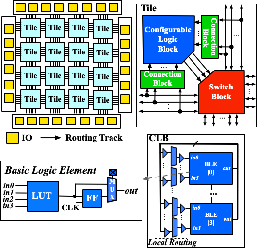
<!-- 
Architecture file translated from ifar repository N04K04L01.FC15FO25.AREA1DELAY1.CMOS90NM.BPTM

Simple architecture file consisting of clusters of 4 BLEs, each BLE contains a 4-LUT+FF pair. Delay models from 90nm PTM.
-->
<architecture>
<!--
ODIN II specific config begins
Describes the types of user-specified netlist blocks (in blif, this corresponds to
".model [type_of_block]") that this architecture supports.

Note: Basic LUTs, I/Os, and flip-flops are not included here as there are
already special structures in blif (.names, .input, .output, and .latch)
that describe them.
-->
<models>
</models>
<tiles>
<tile name="io">
<sub_tile name="io" capacity="3">
<equivalent_sites>
<site pb_type="io" pin_mapping="direct"/>
</equivalent_sites>
<input name="outpad" num_pins="1"/>
<output name="inpad" num_pins="1"/>
<clock name="clock" num_pins="1"/>
<fc in_type="frac" in_val="1.0" out_type="frac" out_val="0.25"/>
<pinlocations pattern="custom">
<loc side="left">io.outpad io.inpad io.clock</loc>
<loc side="top">io.outpad io.inpad io.clock</loc>
<loc side="right">io.outpad io.inpad io.clock</loc>
<loc side="bottom">io.outpad io.inpad io.clock</loc>
</pinlocations>
</sub_tile>
</tile>
<tile name="clb">
<sub_tile name="clb">
<equivalent_sites>
<site pb_type="clb" pin_mapping="direct"/>
</equivalent_sites>
<input name="I" num_pins="10" equivalent="full"/>
<output name="O" num_pins="4" equivalent="instance"/>
<clock name="clk" num_pins="1"/>
<fc in_type="frac" in_val="0.15" out_type="frac" out_val="0.25"/>
<pinlocations pattern="spread"/>
</sub_tile>
</tile>
</tiles>
<!-- ODIN II specific config ends -->
<!-- Physical descriptions begin -->
<layout>
<auto_layout aspect_ratio="1.000000">
<!--Perimeter of 'io' blocks with 'EMPTY' blocks at corners-->
<perimeter type="io" priority="100"/>
<corners type="EMPTY" priority="101"/>
<!--Fill with 'clb'-->
<fill type="clb" priority="10"/>
</auto_layout>
</layout>
<device>
<sizing R_minW_nmos="4220.930176" R_minW_pmos="11207.599609"/>
<area grid_logic_tile_area="2229.320068"/>
<chan_width_distr>
<x distr="uniform" peak="1.000000"/>
<y distr="uniform" peak="1.000000"/>
</chan_width_distr>
<switch_block type="wilton" fs="3"/>
<connection_block input_switch_name="ipin_cblock"/>
</device>
<switchlist>
<switch type="mux" name="0" R="0.000000" Cin="0.000000e+00" Cout="0.000000e+00" Tdel="6.244000e-11" mux_trans_size="1.835460" buf_size="10.498600"/>
<!--switch ipin_cblock resistance set to yeild for 4x minimum drive strength buffer-->
<switch type="mux" name="ipin_cblock" R="1055.232544" Cout="0." Cin="0.000000e+00" Tdel="8.045000e-11" mux_trans_size="0.983352" buf_size="auto"/>
</switchlist>
<segmentlist>
<segment freq="1.000000" length="1" type="unidir" Rmetal="0.000000" Cmetal="0.000000e+00">
<mux name="0"/>
<sb type="pattern">1 1</sb>
<cb type="pattern">1</cb>
</segment>
</segmentlist>
<complexblocklist>
<!-- Define I/O pads begin -->
<!-- Capacity is a unique property of I/Os, it is the maximum number of I/Os that can be placed at the same (X,Y) location on the FPGA -->
<pb_type name="io">
<input name="outpad" num_pins="1"/>
<output name="inpad" num_pins="1"/>
<clock name="clock" num_pins="1"/>
<!-- IOs can operate as either inputs or outputs.
Delays below come from Ian Kuon. They are small, so they should be interpreted as
the delays to and from registers in the I/O (and generally I/Os are registered
today and that is when you timing analyze them.
-->
<mode name="inpad">
<pb_type name="inpad" blif_model=".input" num_pb="1">
<output name="inpad" num_pins="1"/>
</pb_type>
<interconnect>
<direct name="inpad" input="inpad.inpad" output="io.inpad">
<delay_constant max="9.492000e-11" in_port="inpad.inpad" out_port="io.inpad"/>
</direct>
</interconnect>
</mode>
<mode name="outpad">
<pb_type name="outpad" blif_model=".output" num_pb="1">
<input name="outpad" num_pins="1"/>
</pb_type>
<interconnect>
<direct name="outpad" input="io.outpad" output="outpad.outpad">
<delay_constant max="2.675000e-11" in_port="io.outpad" out_port="outpad.outpad"/>
</direct>
</interconnect>
</mode>
<!-- Every input pin is driven by 15% of the tracks in a channel, every output pin is driven by 10% of the tracks in a channel -->
<!-- IOs go on the periphery of the FPGA, for consistency,
make it physically equivalent on all sides so that only one definition of I/Os is needed.
If I do not make a physically equivalent definition, then I need to define 4 different I/Os, one for each side of the FPGA
-->
<!-- Place I/Os on the sides of the FPGA -->
<power method="ignore"/>
</pb_type>
<!-- Define I/O pads ends -->
<!-- Define general purpose logic block (CLB) begin -->
<pb_type name="clb">
<input name="I" num_pins="10" equivalent="full"/>
<output name="O" num_pins="4" equivalent="instance"/>
<clock name="clk" num_pins="1"/>
<!-- Describe basic logic element. -->
<pb_type name="fle" num_pb="4">
<input name="in" num_pins="4"/>
<output name="out" num_pins="1"/>
<clock name="clk" num_pins="1"/>
<!-- 4-LUT mode definition begin -->
<mode name="n1_lut4">
<!-- Define 4-LUT mode -->
<pb_type name="ble4" num_pb="1">
<input name="in" num_pins="4"/>
<output name="out" num_pins="1"/>
<clock name="clk" num_pins="1"/>
<!-- Define LUT -->
<pb_type name="lut4" blif_model=".names" num_pb="1" class="lut">
<input name="in" num_pins="4" port_class="lut_in"/>
<output name="out" num_pins="1" port_class="lut_out"/>
<!-- LUT timing using delay matrix -->
<delay_matrix type="max" in_port="lut4.in" out_port="lut4.out">
2.253000e-10
2.253000e-10
2.253000e-10
2.253000e-10
</delay_matrix>
</pb_type>
<!-- Define flip-flop -->
<pb_type name="ff" blif_model=".latch" num_pb="1" class="flipflop">
<input name="D" num_pins="1" port_class="D"/>
<output name="Q" num_pins="1" port_class="Q"/>
<clock name="clk" num_pins="1" port_class="clock"/>
<T_setup value="2.160000e-10" port="ff.D" clock="clk"/>
<T_clock_to_Q max="1.426000e-10" port="ff.Q" clock="clk"/>
</pb_type>
<interconnect>
<direct name="direct1" input="ble4.in" output="lut4[0:0].in"/>
<direct name="direct2" input="lut4.out" output="ff.D">
<!-- Advanced user option that tells CAD tool to find LUT+FF pairs in netlist -->
<pack_pattern name="ble6" in_port="lut4.out" out_port="ff.D"/>
</direct>
<direct name="direct3" input="ble4.clk" output="ff.clk"/>
<mux name="mux1" input="ff.Q lut4.out" output="ble4.out">
</mux>
</interconnect>
</pb_type>
<interconnect>
<direct name="direct1" input="fle.in" output="ble4.in"/>
<direct name="direct2" input="ble4.out" output="fle.out[0:0]"/>
<direct name="direct3" input="fle.clk" output="ble4.clk"/>
</interconnect>
</mode>
<!-- 4-LUT mode definition end -->
</pb_type>
<interconnect>
<!-- We use a full crossbar to get logical equivalence at inputs of CLB -->
<complete name="crossbar" input="clb.I fle[3:0].out" output="fle[3:0].in">
<delay_constant max="5.735000e-11" in_port="clb.I" out_port="fle[3:0].in"/>
<delay_constant max="5.428000e-11" in_port="fle[3:0].out" out_port="fle[3:0].in"/>
</complete>
<complete name="clks" input="clb.clk" output="fle[3:0].clk">
</complete>
<direct name="clbouts1" input="fle[3:0].out" output="clb.O"/>
</interconnect>
<!-- Every input pin is driven by 15% of the tracks in a channel, every output pin is driven by 25% of the tracks in a channel -->
<!-- Place this general purpose logic block in any unspecified column -->
</pb_type>
<!-- Define general purpose logic block (CLB) ends -->
</complexblocklist>
</architecture>

改变VPR架构

物理IO模型

因为Open FPGA需要物理IO块,而不是抽象的VPR的IO模型,因此需要在<complexblocklist>标签下添加<pb_type name="io">,如一下代码所示

1
2
3
4
5
6
7
8
9
10
11
12
13
14
15
16
17
18
19
20
21
22
23
24
25
26
27
28
29
30
31
32
33
34
35
36
37
38
39
40
41
42
43
44
45
46
<!-- Define I/O pads begin -->
<pb_type name="io">
<input name="outpad" num_pins="1"/>
<output name="inpad" num_pins="1"/>

<!-- A mode denotes the physical implementation of an I/O
This mode will not be used by packer but is mainly used for fabric verilog generation
-->
<mode name="physical" packable="false">
<pb_type name="iopad" blif_model=".subckt io" num_pb="1">
<input name="outpad" num_pins="1"/>
<output name="inpad" num_pins="1"/>
</pb_type>
<interconnect>
<direct name="outpad" input="io.outpad" output="iopad.outpad">
<delay_constant max="1.394e-11" in_port="io.outpad" out_port="iopad.outpad"/>
</direct>
<direct name="inpad" input="iopad.inpad" output="io.inpad">
<delay_constant max="4.243e-11" in_port="iopad.inpad" out_port="io.inpad"/>
</direct>
</interconnect>
</mode>

<!-- Operating modes of I/O used by VPR
IOs can operate as either inputs or outputs. -->
<mode name="inpad">
<pb_type name="inpad" blif_model=".input" num_pb="1">
<output name="inpad" num_pins="1"/>
</pb_type>
<interconnect>
<direct name="inpad" input="inpad.inpad" output="io.inpad">
<delay_constant max="9.492000e-11" in_port="inpad.inpad" out_port="io.inpad"/>
</direct>
</interconnect>
</mode>
<mode name="outpad">
<pb_type name="outpad" blif_model=".output" num_pb="1">
<input name="outpad" num_pins="1"/>
</pb_type>
<interconnect>
<direct name="outpad" input="io.outpad" output="outpad.outpad">
<delay_constant max="2.675000e-11" in_port="io.outpad" out_port="outpad.outpad"/>
</direct>
</interconnect>
</mode>
</pb_type>

与原始的XML相比,主要有以下几点变化:

  1. 添加了physical mode的IO,用于生成fabric网表
  2. 移除了IO的时钟端口(因为实际上是一个悬空端口)
  3. 在physical mode里面使用了属性packable=false,可以降低打包器的运行时间。

由于上述的操作添加了新的BLIF模型subckt io,所以应该在<models>标签下添加一个新的IO模型。如下代码所示:

1
2
3
4
5
6
7
8
9
10
11
<models>
<!-- A virtual model for I/O to be used in the physical mode of io block -->
<model name="io">
<input_ports>
<port name="outpad"/>
</input_ports>
<output_ports>
<port name="inpad"/>
</output_ports>
</model>
</models>

Tileable架构

OpenFPGA 确实支持细粒度的tileable的架构,tileable架构可快速生成网表,并通过后端流程实现高度优化的物理设计。为了使能tileable架构,应该将tileable属性添加到<layout>节点。通过启用此功能,将生成尽可能相同的所有开关块和连接块。因此,对于任何 FPGA 阵列大小,在网表中只生成 9 个独特的块。请参阅[TGAG19]中的详细信息。

1
<layout tileable="true">

OPENFPGA工艺架构

整个IOENFPGA的工艺架构组织如下:

1
2
3
4
5
6
7
8
9
10
11
12
13
14
15
16
17
18
19
20
21
22
23
24
25
26
27
28
29
30
<openfpga_architecture>
<!-- Technology-related (device/transistor-level) information-->
<technology_library>
...
</technology_library>

<!-- Circuit-level description -->
<circuit_library>
...
</circuit_library>

<!-- Configuration protocol definition -->
<configuration_protocol>
...
</configuration_protocol>

<!-- Annotation on VPR architecture modules -->
<connection_block>
...
</connection_block>
<switch_block>
...
</switch_block>
<routing_segment>
...
</routing_segment>
<pb_type_annotations>
...
</pb_type_annotations>
</openfpga_architecture>

technology library

此部分包含了构建FPGA的晶体管级的信息,这对于FPGA-SPICE来生成网表来说是很重要的,但是如果不适用FPGA-SPICE,就可以提供虚拟的(dummy)technology library。

open-source ASU Predictive Technology Modeling (PTM) 45nm process library的xml描述如下所示:

1
2
3
4
5
6
7
8
9
10
11
12
13
14
15
16
17
18
19
20
<technology_library>
<device_library>
<device_model name="logic" type="transistor">
<lib type="industry" corner="TOP_TT" ref="M" path="${OPENFPGA_PATH}/openfpga_flow/tech/PTM_45nm/45nm.pm"/>
<design vdd="0.9" pn_ratio="2"/>
<pmos name="pch" chan_length="40e-9" min_width="140e-9" variation="logic_transistor_var"/>
<nmos name="nch" chan_length="40e-9" min_width="140e-9" variation="logic_transistor_var"/>
</device_model>
<device_model name="io" type="transistor">
<lib type="academia" ref="M" path="${OPENFPGA_PATH}/openfpga_flow/tech/PTM_45nm/45nm.pm"/>
<design vdd="2.5" pn_ratio="3"/>
<pmos name="pch_25" chan_length="270e-9" min_width="320e-9" variation="io_transistor_var"/>
<nmos name="nch_25" chan_length="270e-9" min_width="320e-9" variation="io_transistor_var"/>
</device_model>
</device_library>
<variation_library>
<variation name="logic_transistor_var" abs_deviation="0.1" num_sigma="3"/>
<variation name="io_transistor_var" abs_deviation="0.1" num_sigma="3"/>
</variation_library>
</technology_library>

circuit library

circuit library是架构描述的关键部件,包含了一系列的<circuit_model>,每一个都描述了FPGA部件是如何电路实现的。通常的实现过程中会先描述一部分原子模型,然后通过原子模型来描述基元模型,而基元模型则直接用来构建FPGA组件(LUT等)。

以下的参考代码描述了反相器、缓冲器以及传输门等原子逻辑:

1
2
3
4
5
6
7
8
9
10
11
12
13
14
15
16
17
18
19
20
21
22
23
24
25
26
27
28
29
30
31
32
33
34
35
36
37
38
39
40
41
42
43
44
45
46
47
48
49
50
51
52
53
54
55
56
57
58
59
60
61
62
63
64
65
66
<!-- Atom circuit models begin-->
<circuit_model type="inv_buf" name="INVTX1" prefix="INVTX1" is_default="true">
<design_technology type="cmos" topology="inverter" size="1"/>
<port type="input" prefix="in" size="1"/>
<port type="output" prefix="out" size="1"/>
<delay_matrix type="rise" in_port="in" out_port="out">
10e-12
</delay_matrix>
<delay_matrix type="fall" in_port="in" out_port="out">
10e-12
</delay_matrix>
</circuit_model>
<circuit_model type="inv_buf" name="buf4" prefix="buf4" is_default="false">
<design_technology type="cmos" topology="buffer" size="1" num_level="2" f_per_stage="4"/>
<port type="input" prefix="in" size="1"/>
<port type="output" prefix="out" size="1"/>
<delay_matrix type="rise" in_port="in" out_port="out">
10e-12
</delay_matrix>
<delay_matrix type="fall" in_port="in" out_port="out">
10e-12
</delay_matrix>
</circuit_model>
<circuit_model type="inv_buf" name="tap_buf4" prefix="tap_buf4" is_default="false">
<design_technology type="cmos" topology="buffer" size="1" num_level="3" f_per_stage="4"/>
<port type="input" prefix="in" size="1"/>
<port type="output" prefix="out" size="1"/>
<delay_matrix type="rise" in_port="in" out_port="out">
10e-12
</delay_matrix>
<delay_matrix type="fall" in_port="in" out_port="out">
10e-12
</delay_matrix>
</circuit_model>
<circuit_model type="pass_gate" name="TGATE" prefix="TGATE" is_default="true">
<design_technology type="cmos" topology="transmission_gate" nmos_size="1" pmos_size="2"/>
<input_buffer exist="false"/>
<output_buffer exist="false"/>
<port type="input" prefix="in" size="1"/>
<port type="input" prefix="sel" size="1"/>
<port type="input" prefix="selb" size="1"/>
<port type="output" prefix="out" size="1"/>
<delay_matrix type="rise" in_port="in sel selb" out_port="out">
10e-12 5e-12 5e-12
</delay_matrix>
<delay_matrix type="fall" in_port="in sel selb" out_port="out">
10e-12 5e-12 5e-12
</delay_matrix>
</circuit_model>
<circuit_model type="chan_wire" name="chan_segment" prefix="track_seg" is_default="true">
<design_technology type="cmos"/>
<input_buffer exist="false"/>
<output_buffer exist="false"/>
<port type="input" prefix="in" size="1"/>
<port type="output" prefix="out" size="1"/>
<wire_param model_type="pi" R="101" C="22.5e-15" num_level="1"/> <!-- model_type could be T, res_val and cap_val DON'T CARE -->
</circuit_model>
<circuit_model type="wire" name="direct_interc" prefix="direct_interc" is_default="true">
<design_technology type="cmos"/>
<input_buffer exist="false"/>
<output_buffer exist="false"/>
<port type="input" prefix="in" size="1"/>
<port type="output" prefix="out" size="1"/>
<wire_param model_type="pi" R="0" C="0" num_level="1"/> <!-- model_type could be T, res_val cap_val should be defined -->
</circuit_model>
<!-- Atom circuit models end-->

在以下实例代码中描述了布线多路选择器、LUT以及IO cells等基元模型。其中static_diffsc_dff_compact以及iopad需要手动指定Verilog网表,而其他电路模型则可以通过OpenFPGA自动生成。

1
2
3
4
5
6
7
8
9
10
11
12
13
14
15
16
17
18
19
20
21
22
23
24
25
26
27
28
29
30
31
32
33
34
35
36
37
38
39
40
41
42
43
44
45
46
47
48
49
50
51
52
53
54
55
56
57
58
59
60
61
62
63
64
65
66
67
68
69
70
71
<!-- Primitive circuit models begin -->
<circuit_model type="mux" name="mux_2level" prefix="mux_2level" dump_structural_verilog="true">
<design_technology type="cmos" structure="multi_level" num_level="2" add_const_input="true" const_input_val="1"/>
<input_buffer exist="true" circuit_model_name="INVTX1"/>
<output_buffer exist="true" circuit_model_name="INVTX1"/>
<pass_gate_logic circuit_model_name="TGATE"/>
<port type="input" prefix="in" size="1"/>
<port type="output" prefix="out" size="1"/>
<port type="sram" prefix="sram" size="1"/>
</circuit_model>
<circuit_model type="mux" name="mux_2level_tapbuf" prefix="mux_2level_tapbuf" dump_structural_verilog="true">
<design_technology type="cmos" structure="multi_level" num_level="2" add_const_input="true" const_input_val="1"/>
<input_buffer exist="true" circuit_model_name="INVTX1"/>
<output_buffer exist="true" circuit_model_name="tap_buf4"/>
<pass_gate_logic circuit_model_name="TGATE"/>
<port type="input" prefix="in" size="1"/>
<port type="output" prefix="out" size="1"/>
<port type="sram" prefix="sram" size="1"/>
</circuit_model>
<circuit_model type="mux" name="mux_1level_tapbuf" prefix="mux_1level_tapbuf" is_default="true" dump_structural_verilog="true">
<design_technology type="cmos" structure="one_level" add_const_input="true" const_input_val="1"/>
<input_buffer exist="true" circuit_model_name="INVTX1"/>
<output_buffer exist="true" circuit_model_name="tap_buf4"/>
<pass_gate_logic circuit_model_name="TGATE"/>
<port type="input" prefix="in" size="1"/>
<port type="output" prefix="out" size="1"/>
<port type="sram" prefix="sram" size="1"/>
</circuit_model>
<!--DFF subckt ports should be defined as <D> <Q> <CLK> <RESET> <SET> -->
<circuit_model type="ff" name="static_dff" prefix="dff" spice_netlist="${OPENFPGA_PATH}/openfpga_flow/SpiceNetlists/ff.sp" verilog_netlist="${OPENFPGA_PATH}/openfpga_flow/VerilogNetlists/ff.v">
<design_technology type="cmos"/>
<input_buffer exist="true" circuit_model_name="INVTX1"/>
<output_buffer exist="true" circuit_model_name="INVTX1"/>
<port type="input" prefix="D" size="1"/>
<port type="input" prefix="set" size="1" is_global="true" default_val="0" is_set="true"/>
<port type="input" prefix="reset" size="1" is_global="true" default_val="0" is_reset="true"/>
<port type="output" prefix="Q" size="1"/>
<port type="clock" prefix="clk" size="1" is_global="true" default_val="0" />
</circuit_model>
<circuit_model type="lut" name="lut4" prefix="lut4" dump_structural_verilog="true">
<design_technology type="cmos"/>
<input_buffer exist="true" circuit_model_name="INVTX1"/>
<output_buffer exist="true" circuit_model_name="INVTX1"/>
<lut_input_inverter exist="true" circuit_model_name="INVTX1"/>
<lut_input_buffer exist="true" circuit_model_name="buf4"/>
<pass_gate_logic circuit_model_name="TGATE"/>
<port type="input" prefix="in" size="4"/>
<port type="output" prefix="out" size="1"/>
<port type="sram" prefix="sram" size="16"/>
</circuit_model>
<!--Scan-chain DFF subckt ports should be defined as <D> <Q> <Qb> <CLK> <RESET> <SET> -->
<circuit_model type="ccff" name="sc_dff_compact" prefix="scff" spice_netlist="${OPENFPGA_PATH}/openfpga_flow/SpiceNetlists/ff.sp" verilog_netlist="${OPENFPGA_PATH}/openfpga_flow/VerilogNetlists/ff.v">
<design_technology type="cmos"/>
<input_buffer exist="true" circuit_model_name="INVTX1"/>
<output_buffer exist="true" circuit_model_name="INVTX1"/>
<port type="input" prefix="pReset" lib_name="reset" size="1" is_global="true" default_val="0" is_reset="true" is_prog="true"/>
<port type="input" prefix="D" size="1"/>
<port type="output" prefix="Q" size="1"/>
<port type="output" prefix="Qb" size="1"/>
<port type="clock" prefix="prog_clk" lib_name="clk" size="1" is_global="true" default_val="0" is_prog="true"/>
</circuit_model>
<circuit_model type="iopad" name="iopad" prefix="iopad" spice_netlist="${OPENFPGA_PATH}/openfpga_flow/SpiceNetlists/io.sp" verilog_netlist="${OPENFPGA_PATH}/openfpga_flow/VerilogNetlists/io.v">
<design_technology type="cmos"/>
<input_buffer exist="true" circuit_model_name="INVTX1"/>
<output_buffer exist="true" circuit_model_name="INVTX1"/>
<port type="inout" prefix="pad" size="1" is_global="true" is_io="true"/>
<port type="sram" prefix="en" size="1" mode_select="true" circuit_model_name="sc_dff_compact" default_val="1"/>
<port type="input" prefix="outpad" size="1"/>
<port type="output" prefix="inpad" size="1"/>
</circuit_model>
<!-- Primitive circuit models end -->

配置协议定义

以下代码指定 FPGA 架构将通过一系列触发器 (FF) 进行配置,该触发器使用.<circuit_model name=sc_dff_compact>

1
2
3
<configuration_protocol>
<organization type="scan_chain" circuit_model_name="sc_dff_compact"/>
</configuration_protocol>

对VPR模型进行标注

对于路由架构,需要指定连接块、开关快内使用的多路选择器的circuit_model以及布线导线的circuit_model

1
2
3
4
5
6
7
8
9
<connection_block>
<switch name="ipin_cblock" circuit_model_name="mux_2level_tapbuf"/>
</connection_block>
<switch_block>
<switch name="0" circuit_model_name="mux_2level_tapbuf"/>
</switch_block>
<routing_segment>
<segment name="L4" circuit_model_name="chan_segment"/>
</routing_segment>

为了获得正确的绑定,连接块、交换机块和路由段的名称应与 VPR 体系结构描述中的名称定义相匹配!

对于在<comlpexblocklist>中定义的每一个pb_type如果包含多个模式,则应该指定物理模式(physical mode),并且这个物理模块的名字应该与VPR架构中定义的模式名字相匹配。

1
<pb_type name="io" physical_mode_name="physical"/>

在物理模式下,当要指定任何基元pb_type所使用的实现方式(circuit model),需要提供pb_type的详细层次结构。

1
<pb_type name="io[physical].iopad" circuit_model_name="iopad" mode_bits="1"/>

对于可配置资源,应该提供默认的配置比特。例如正如cirtuit_model name=iopad中所定义的一样,IO cell有一个配置比特

对于物理模式以外的其他模式(操作模式),则应该提供从操作模式到物理模式的映射,以至于能够生成比特流。这一步也需要提供pb_type的完整层次结构。

1
<pb_type name="io[inpad].inpad" physical_pb_type_name="io[physical].iopad" mode_bits="1"/>

上述代码就指明了当配置位为1时,被配置为输入模式(应该与io的实现代码有关,有待求证)。

以下代码用于指定用于实现互联模块的电路模型,其中name应该与VPR中的定义相匹配(如果未指定,则会使用默认的circuit_model

1
<interconnect name="crossbar" circuit_model_name="mux_2level"/>

OpenFPGA能自动推断每一个interconnect所需要的circuit model

总感觉与上面的话矛盾!!!

整个完整的标注如下所示:

1
2
3
4
5
6
7
8
9
10
11
12
13
14
15
16
17
18
<pb_type_annotations>
<!-- physical pb_type binding in complex block IO -->
<pb_type name="io" physical_mode_name="physical"/>
<pb_type name="io[physical].iopad" circuit_model_name="iopad" mode_bits="1"/>
<pb_type name="io[inpad].inpad" physical_pb_type_name="io[physical].iopad" mode_bits="1"/>
<pb_type name="io[outpad].outpad" physical_pb_type_name="io[physical].iopad" mode_bits="0"/>
<!-- End physical pb_type binding in complex block IO -->

<!-- physical pb_type binding in complex block CLB -->
<!-- physical mode will be the default mode if not specified -->
<pb_type name="clb">
<!-- Binding interconnect to circuit models as their physical implementation, if not defined, we use the default model -->
<interconnect name="crossbar" circuit_model_name="mux_2level"/>
</pb_type>
<pb_type name="clb.fle[n1_lut4].ble4.lut4" circuit_model_name="lut4"/>
<pb_type name="clb.fle[n1_lut4].ble4.ff" circuit_model_name="static_dff"/>
<!-- End physical pb_type binding in complex block IO -->
</pb_type_annotations>

仿真设置

OpenFPGA需要一个xml文件详细描述仿真设置,仿真设置中包含了用于构建验证testbench的重要参数。本例子的(第一幅图)的仿真设置如下:

1
2
3
4
5
6
7
8
9
10
11
12
13
14
15
16
17
18
19
20
21
22
23
24
25
26
27
28
29
30
31
32
33
<openfpga_simulation_setting>
<clock_setting>
<operating frequency="auto" num_cycles="auto" slack="0.2"/>
<programming frequency="100e6"/>
</clock_setting>
<simulator_option>
<operating_condition temperature="25"/>
<output_log verbose="false" captab="false"/>
<accuracy type="abs" value="1e-13"/>
<runtime fast_simulation="true"/>
</simulator_option>
<monte_carlo num_simulation_points="2"/>
<measurement_setting>
<slew>
<rise upper_thres_pct="0.95" lower_thres_pct="0.05"/>
<fall upper_thres_pct="0.05" lower_thres_pct="0.95"/>
</slew>
<delay>
<rise input_thres_pct="0.5" output_thres_pct="0.5"/>
<fall input_thres_pct="0.5" output_thres_pct="0.5"/>
</delay>
</measurement_setting>
<stimulus>
<clock>
<rise slew_type="abs" slew_time="20e-12" />
<fall slew_type="abs" slew_time="20e-12" />
</clock>
<input>
<rise slew_type="abs" slew_time="25e-12" />
<fall slew_type="abs" slew_time="25e-12" />
</input>
</stimulus>
</openfpga_simulation_setting>

其中<clock_setting>用于在testbench中创建时钟信号。

FPGA有两种类型的时钟,一种是操作时钟,用于控制部署到FPGA fabric中的应用。另一个是编程时钟,用于控制配置协议

<simulator_option>是用于SPICE仿真的选项

感觉暂时用不到

详情请见仿真设置